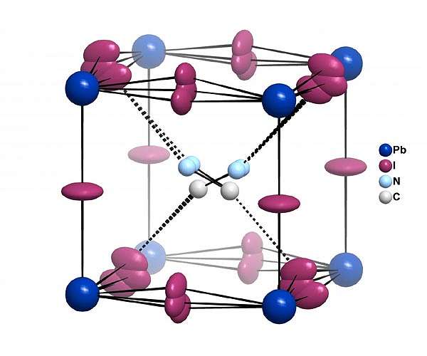
Migrating ions through the perovskite layer in two dimensions
by Staff Writers
Changchun, China (SPX) Apr 13, 2023
Electrostatic doping has been widely used in low-dimensional materials, including carbon nanotube (CNT) and two-dimensional (2D) materials such as graphene and transition metal dichalcogenides (TMDs). Unlike conventional lattice doping with impurity atoms, it is challenging to achieve doping in nanoscale materials due to the limited physical space. The electrostatic doping opens an effective pathway to tune the charge carriers in nanoscale materials without introducing impurity atoms which can perturb the atomic arrangement and degrade the intrinsic electronic properties of the nanoscale materials.
In a new paper published in eLight, a team of scientists led by Professors Sung-Joon Lee and Hung-Chieh Cheng from the University of California Los Angeles has developed a methylammonium lead iodide perovskite (CH3NH3PbI3)/2DSC heterojunction device.
Recently, ionic solids have been explored for creating a p-n junction in monolayer 2D materials. The frozen mobile ions provide electrostatic fields to modulate the carrier density of underlying 2D semiconducting channel. Due to the well-defined shape of ionic solids, local control of the doping on 2D semiconductors (2DSCs) allows diverse designs to integrate solid-state electronic/optoelectronic devices with minimum crosstalk. The manipulation of silver ions in solid-state superionic silver iodide (AgI) was employed for tailoring the carrier type of 2DSCs to achieve reversibly programmable transistors, diodes, photodiodes and logic gates.
The monolayer TMDs have been widely adopted in novel optoelectronic applications such as electrically tunable light-emitting diodes (LEDs), gate-controlled p-n junction diodes, and solar cells. However, the monolayer TMDs exhibit some intrinsic limits for high-performance optoelectronic applications. The incorporation of impurity dopants in the atomically thin 2D lattices has been fundamentally limited by the physical space in the atomically thin lattices.
It has been a persistent challenge to tailor the charge doping type/density in monolayer 2DSCs using selected lattice dopants. Consequently, the p-n photodiodes made from 2DSCs are often plagued by non-ideal contacts at either p- or nside, limiting the achievable open circuit voltage (VOC). Additionally, the total light absorption and spectral sensitivity of 2DSCs are fundamentally limited by their atomically thin geometry. It compromises the photocarrier generation efficiency and the achievable external quantum efficiency (EQE).
Considerable efforts have been devoted to overcoming such intrinsic limitations by heterogeneously integrating with other well-known optoelectronic materials. For example, interfacing with organic dye molecules has been demonstrated as an effective strategy to control its optoelectrical properties. Hybrid lead halide perovskites (LHPs) have received substantial attention for photovoltaics due to their excellent optoelectronic performance and low fabrication cost.
Despite its extraordinary potential, the “soft lattice” ionic LHPs are typically plagued with ion migrations under voltage bias, leading to poor material stability and large hysteresis in the voltage-dependent photocurrents. The migration of positively or negatively charged ions could induce ion accumulation or ionic charge imbalance under applied electric fields. Here, we exploit such ionic charge imbalance in LHPs to induce reversible doping in nearby 2DSCs to create high-performance photodiodes.
Methylammonium lead iodide (CH3NH3PbI3 or MAPbI3) represents the most prominent example of LHPs with excellent optical absorption and photoresponsive properties but is seriously plagued by ionic motion. Although undesirable for stable operation of solar cell applications, the accumulation of ionic charge from the bias-induced ions migration in MAPbI3 can be exploited for selectively doping nearby 2DSCs to create perovskite-sensitized 2D photodiodes with high optoelectronic performance.
In this regard, the atomically thin 2DSCs are ideally suited for efficient coupling with the ionic solids. They serve as a non-covalent doping agent to reversibly induce the reconfigurable p-type or n-type doping effect. Such tunable doping effect further offers a new class of 2DSC-based photodiodes with switchable polarities. With van der Waals integration of ionic solids with excellent optoelectronic properties, the 2D diodes formed from the ionic-doping effect provide an efficient way to extract photogenerated carriers in MAPbI3.
Research Report:Lead halide perovskite sensitized WSe2 photodiodes with ultrahigh open circuit voltages
Related Links
Changchun Institute of Optics, Fine Mechanics And Physics
All About Solar Energy at SolarDaily.com


